Comberry

+7 (8422) 37 01 01

ACCELERATED RESEARCH & DEVELOPMENT

COMBERRY
PLATFORM

A revolutionary approach for accelerating research and development
in functional thin-film coatings, implementing innovations,
and reducing time to market

COMBERRY

Technology for thin-film coatings development

Innovative HPC® platform - a fundamentally new approach

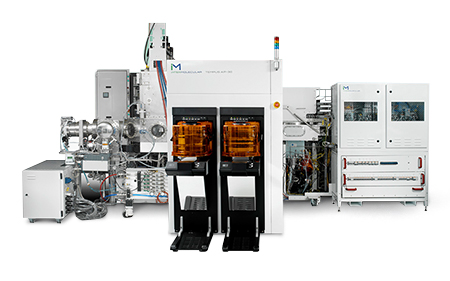
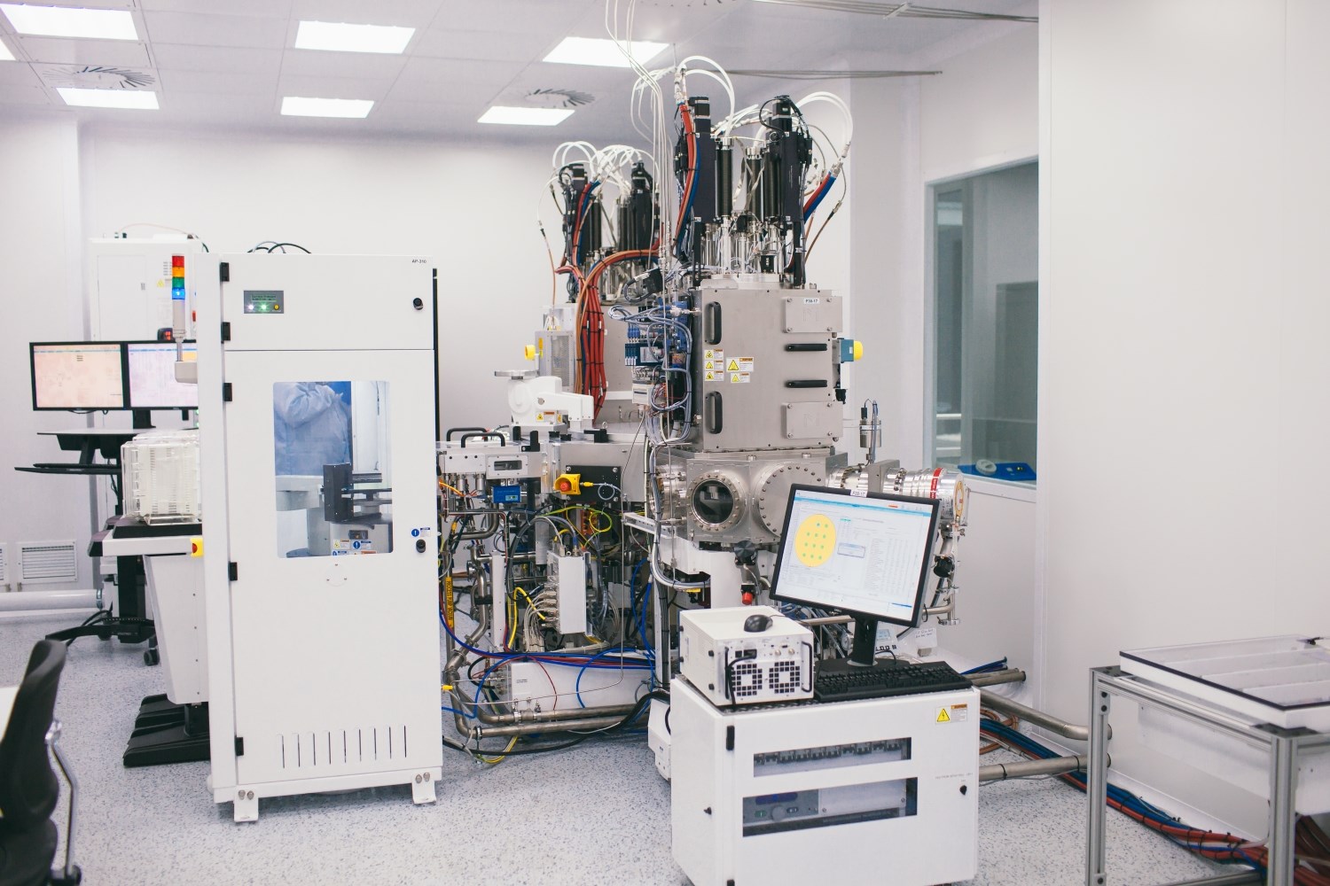
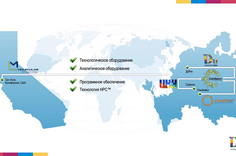
The Comberry™ platform combines software, technological and analytical equipment, and HPC® technology (HPC® technology makes it possible to conduct dozens and even hundreds of experiments simultaneously, thereby discovering the most high-performing materials and their application methods) developed by Intermolecular, Inc. (Intermolecular, Inc. is a research company established in 2004 in California. One of the company’s areas of expertise is creation of a combinatorial (HPC™) platform that accelerates scientific research, implements innovations, and substantially reduces time to market for new products in the semiconductor and clean energy industries.

Within collaborative development research programs (CDPs) implemented jointly with customers, Intermolecular, Inc. creates unique technologies focused on advanced materials and processes.
Intermolecular, Inc. was founded in 2004 in San Jose, California.

All rights to the trademarks “Intermolecular”, “HPC” and the logo of Intermolecular, Inc. are reserved and belong to Intermolecular, Inc.

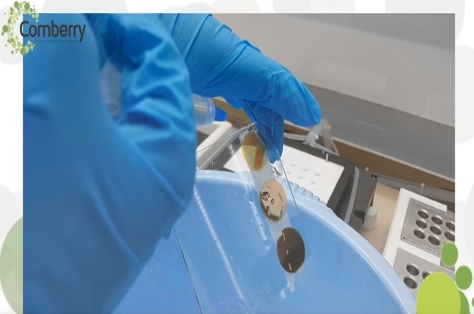
The platform gives the possibility to conduct groups of experiments simultaneously, the results are quickly studied with special analytical methods to determine the most promising materials and processes for fabrication of thin-film devices. Using the platform it is possible to scale up the scientific results from the labs for production.
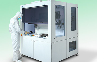
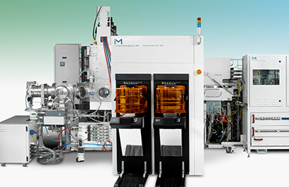
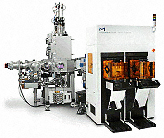
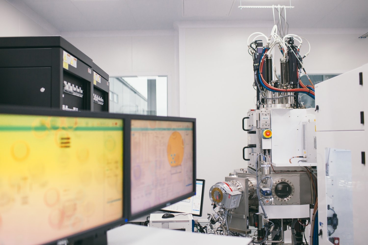
The Comberry ™ Combinatorial Research Platform                            The Comberry ™ Combinatorial Research Platform

Combinatorial technology for thin-film coatings multiplies research cycles and increases their efficiency, which in turn contributes to cost efficient and seamless implementation of innovative solutions to mass production.

The Comberry ™ technology platform is unparalleled in both Russian and European markets.

Innovative HPC® platform - a fundamentally new approach

Technical infrastructure

Equipment

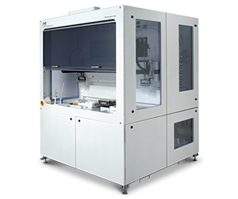
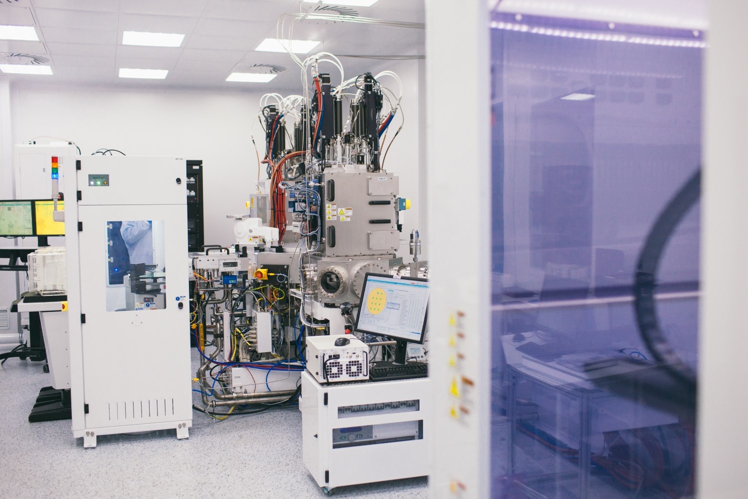
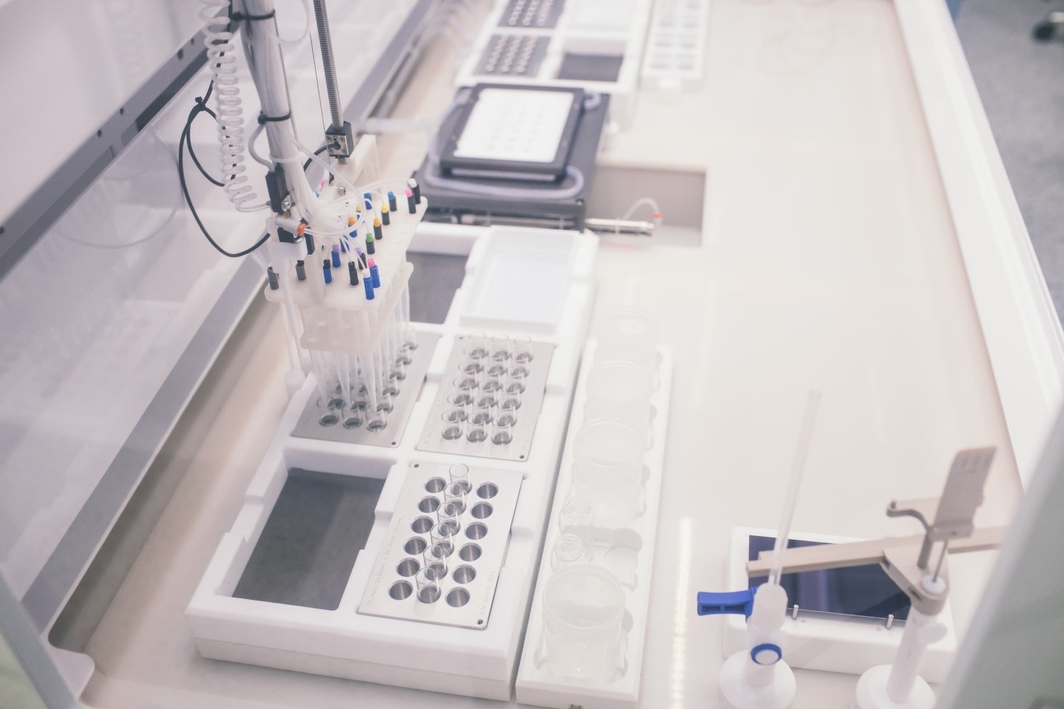
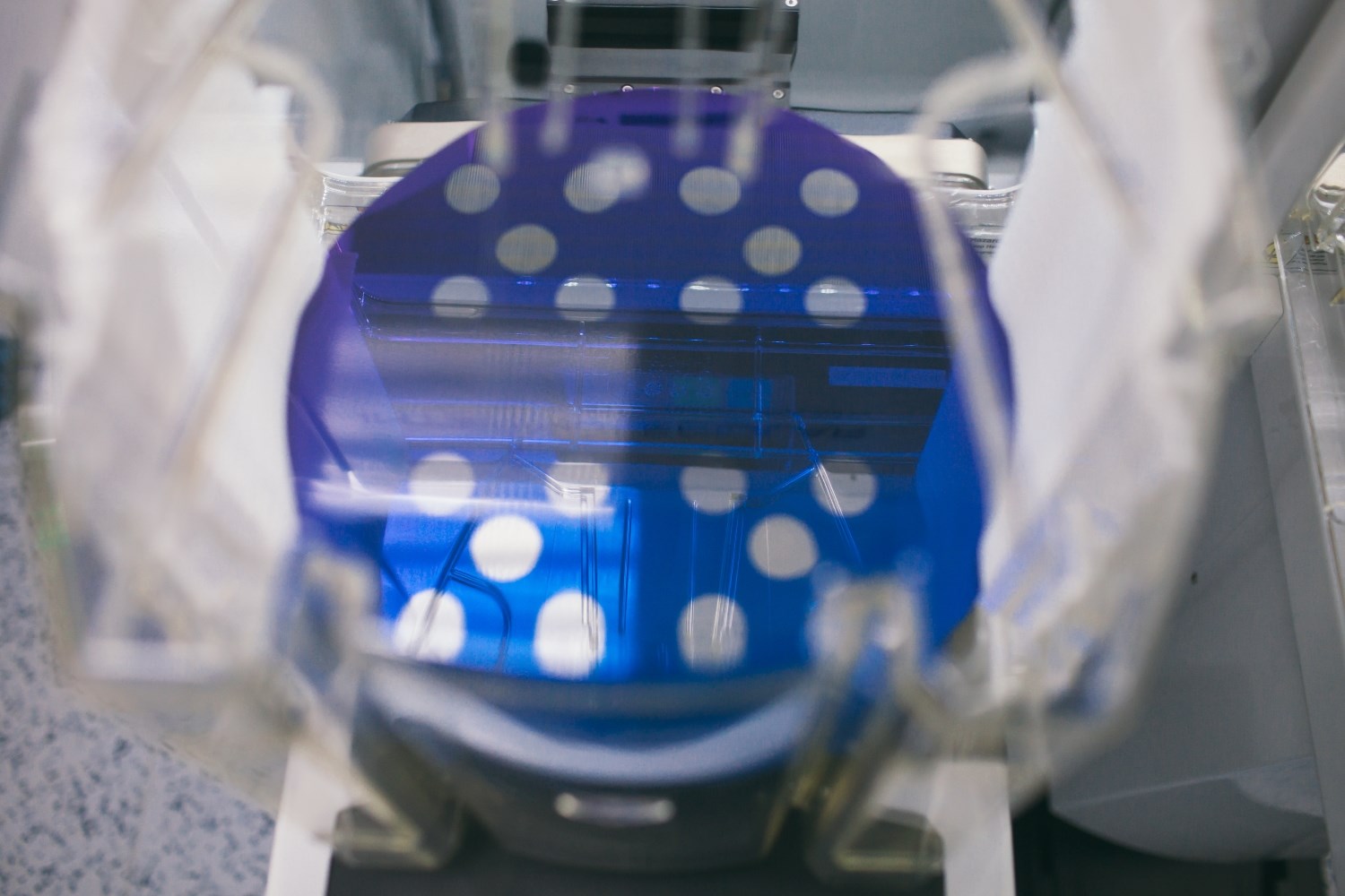
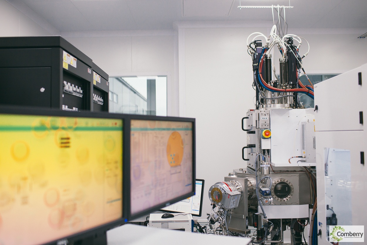
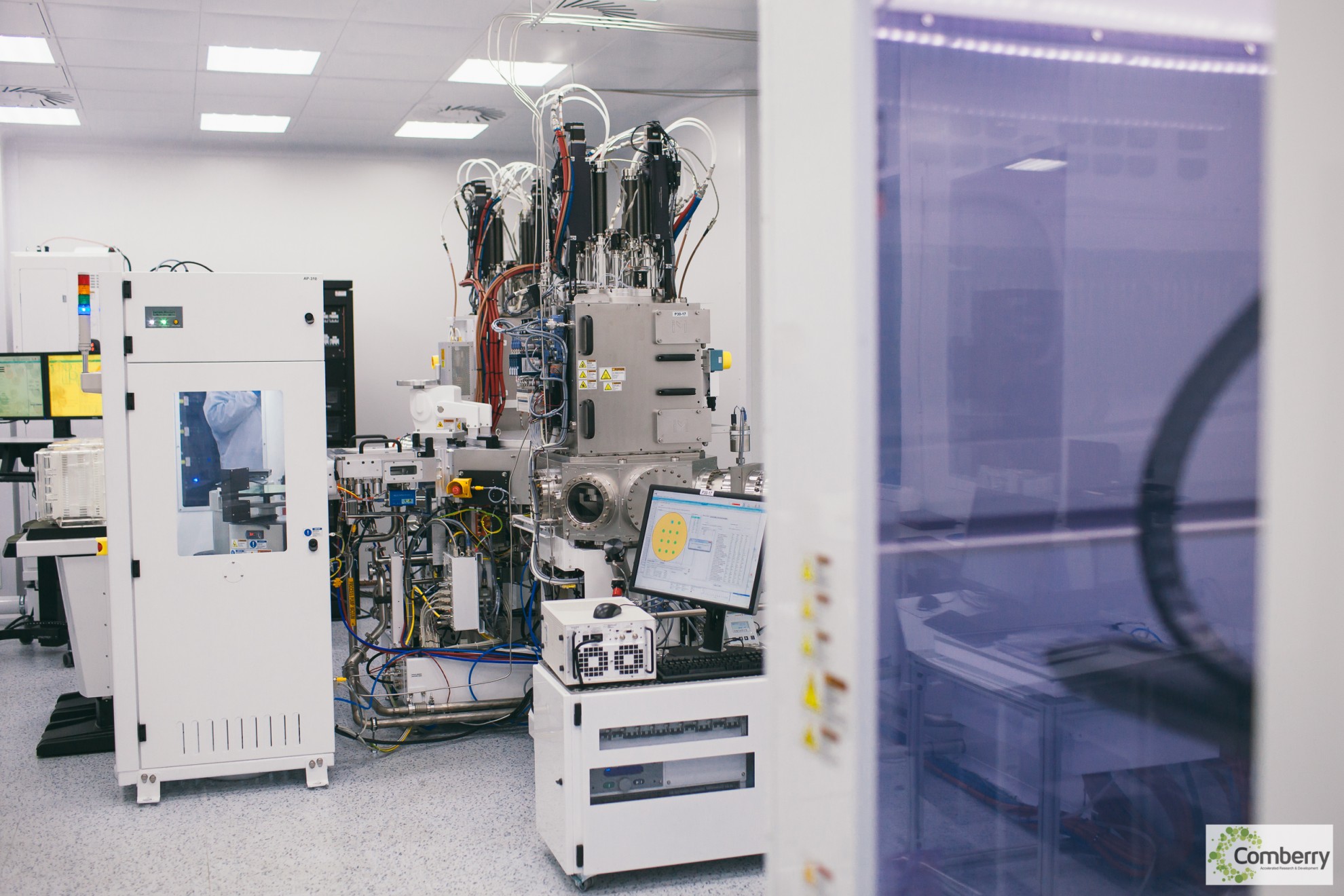
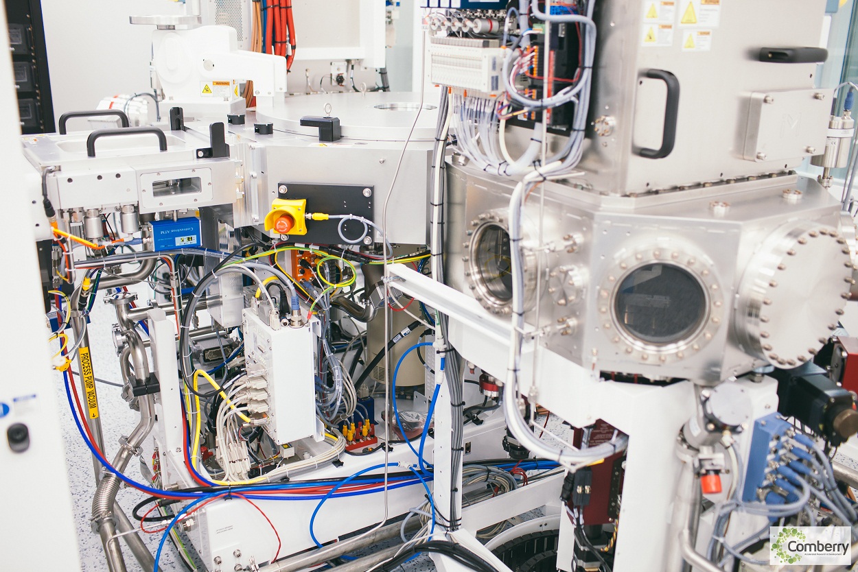
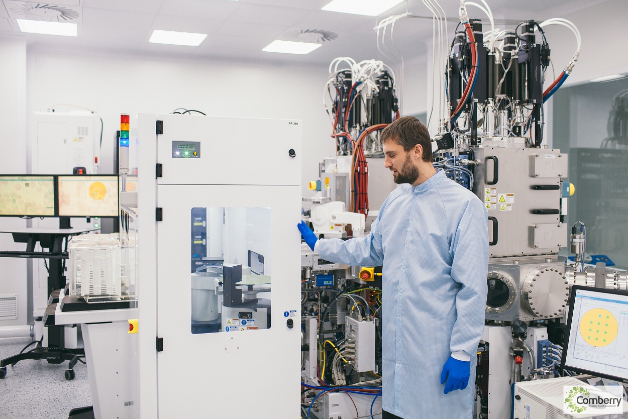
The Comberry ™ Integrated Platform enables significant improvement the efficiency of each stage in the R&D efforts around application of thin-film coatings via Physical Vapor Deposition (PVD, magnetron sputtering ), as well as Liquid-Phase Deposition (LPD) methods. The Platform allows for a wide spectrum of research opportunities in the field of Materials Science of thin-films and optimization of the existing technological processes.

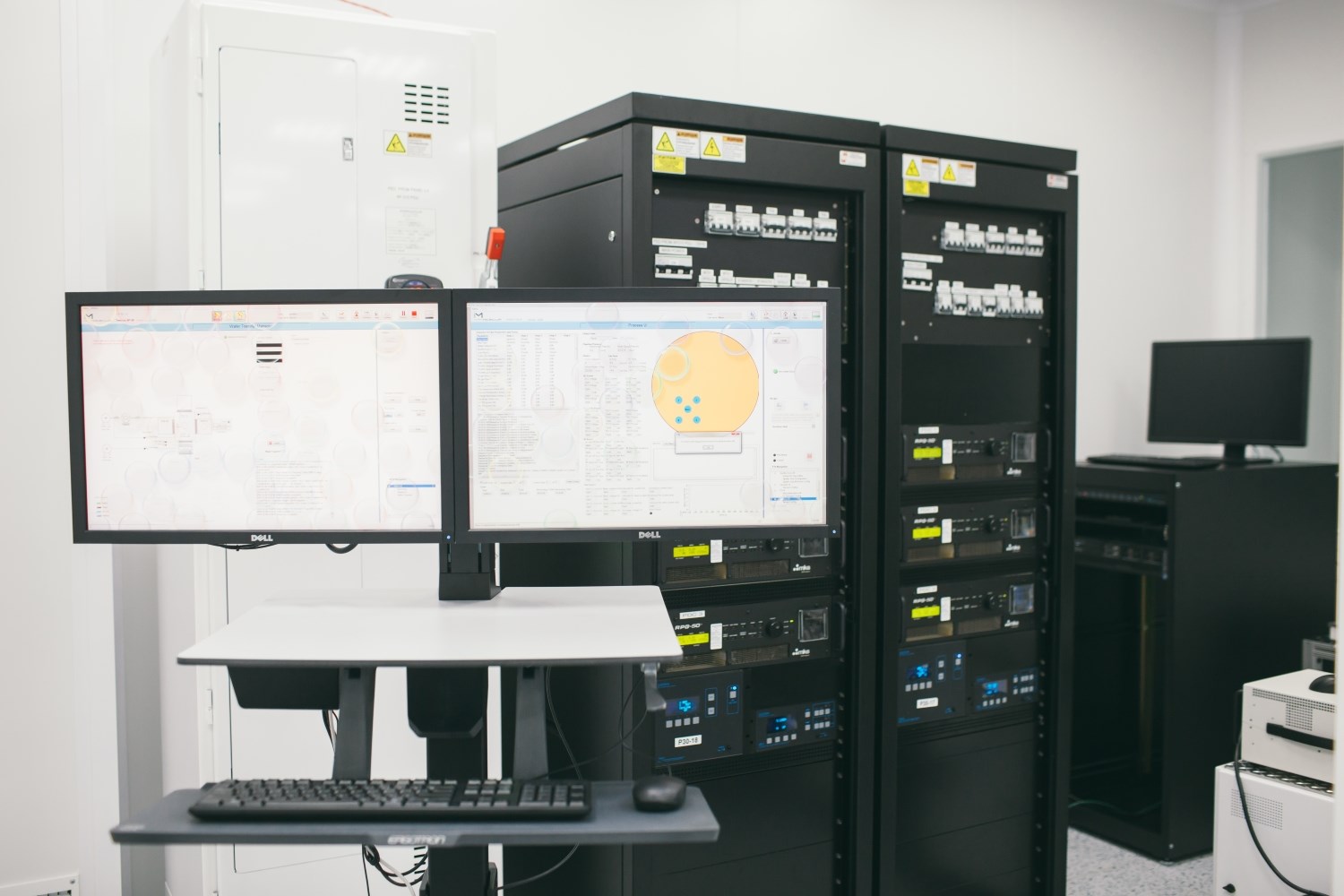
The Integrated R&D Platform HPC® of Comberry includes the following modules:

Laboratory

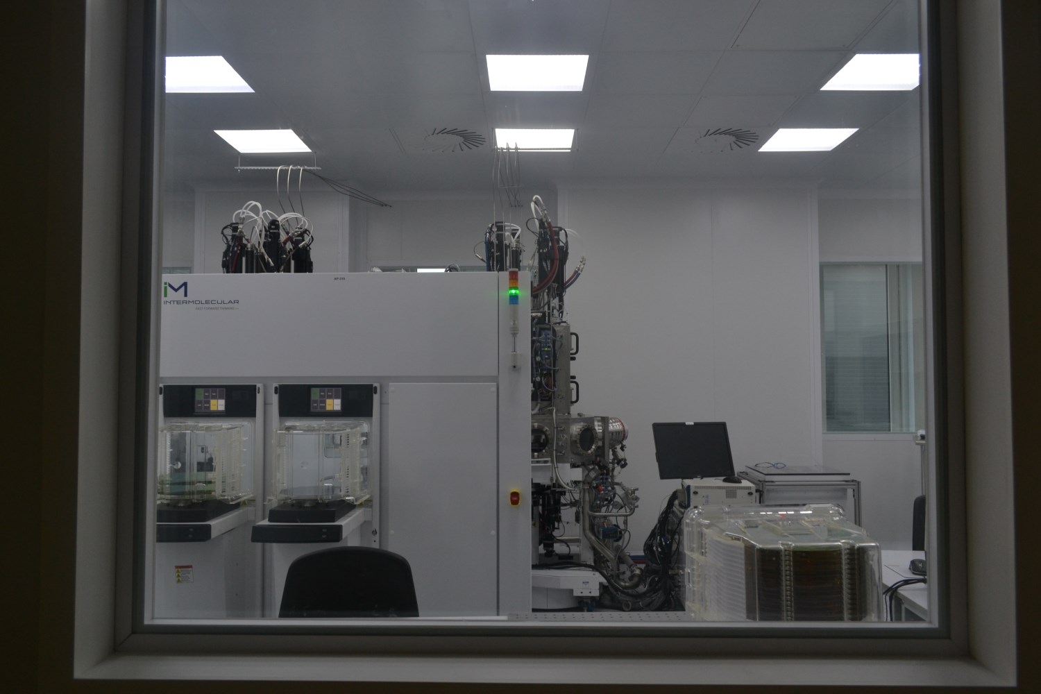
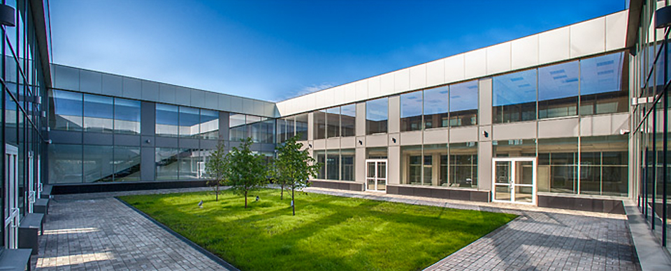
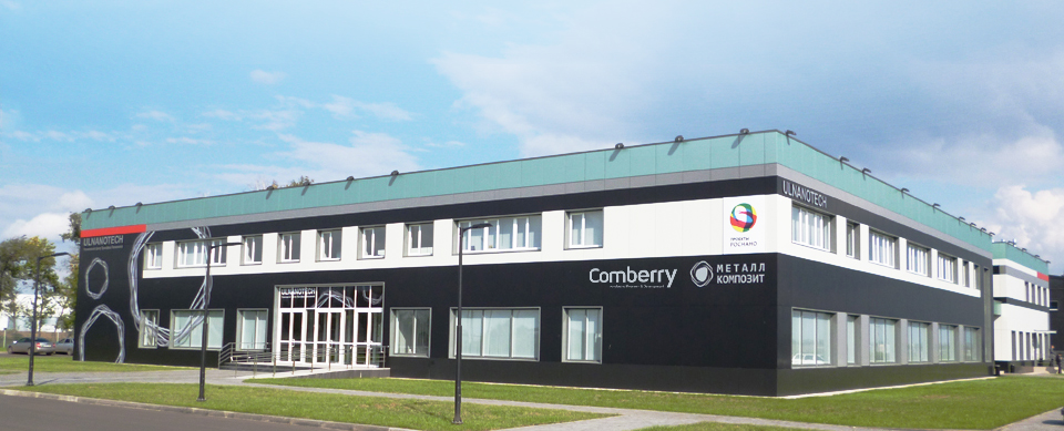
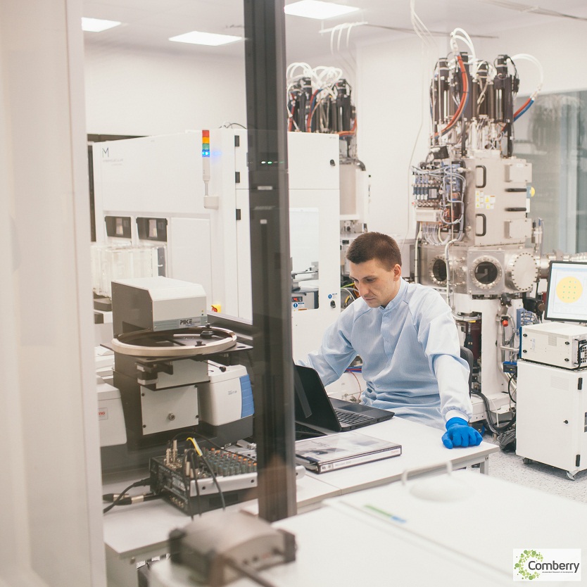
The main technological facility is located in the laboratory of the ULNANOTECH Nanocenter (city of Ulyanovsk).

Comberry™ utilizes the infrastructure and competencies of the Dubna Nanocenter in electrochromic, hydrophobic and hydrophilic adhesive materials as well as the infrastructure of the Saransk Nanocenter in power electronics

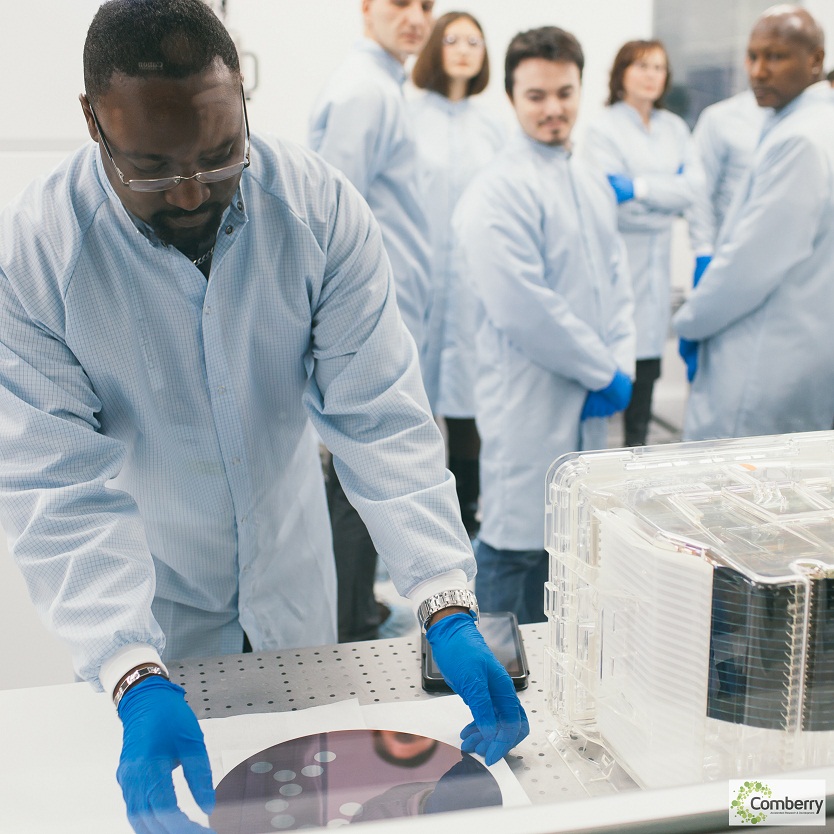
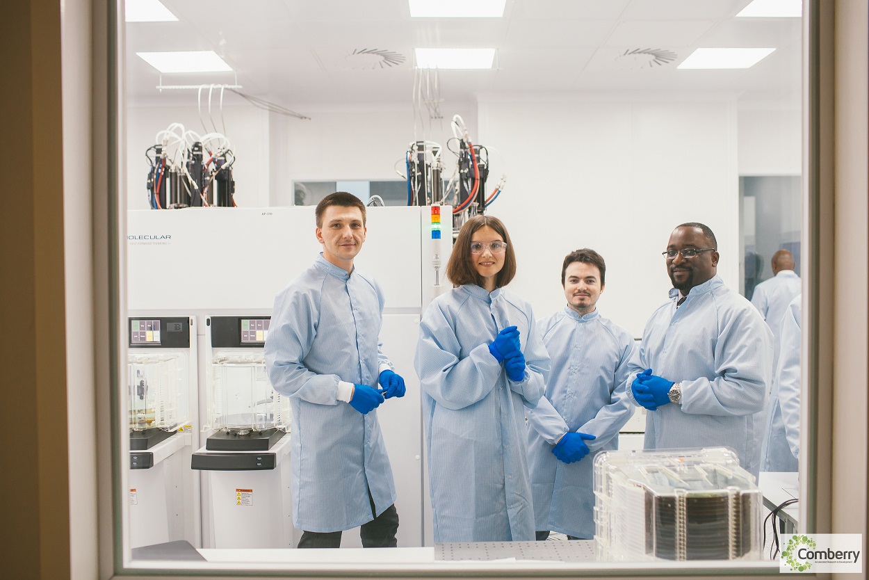
Comberry’s laboratory is a cleanroom  that meets ISO Class 7 requirements.

APPLICATIONS

SERVICES DEVELOPMENT AND DEPOSITION OF MULTIFUNCTIONAL THIN-FILM COATINGS

CUSTOMIZED DEPOSITION

Comberry™ provides comprehensive material characterization and analytical services in the area of thin-film functional coatings.

The Comberry™ highly qualified team using the technological platform contributes to acceleration of developments, depth of understanding and invention of new materials. The Comberry™ engineers provide a thorough customer support at every stage of development - from rapid material deposition and characterization to development programs.


COMBERRY

Collaboration

Comberry ™   invites interested companies to address their problems of how to reduce financial costs and time to search for advanced technology solutions.

Comberry™ invites all interested companies to solve their challenges in order to reduce time and financial costs of finding advanced technological solutions. 

The Comberry TM infrastructure can be used by customers under the contract:

Development of thin-film coatings and devices

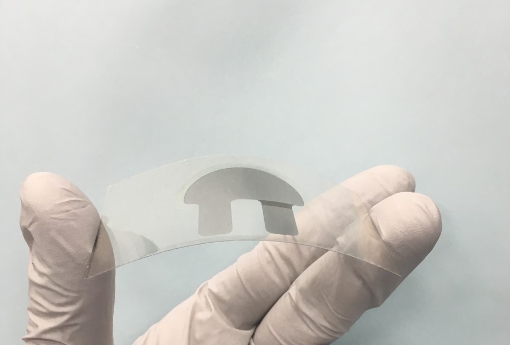
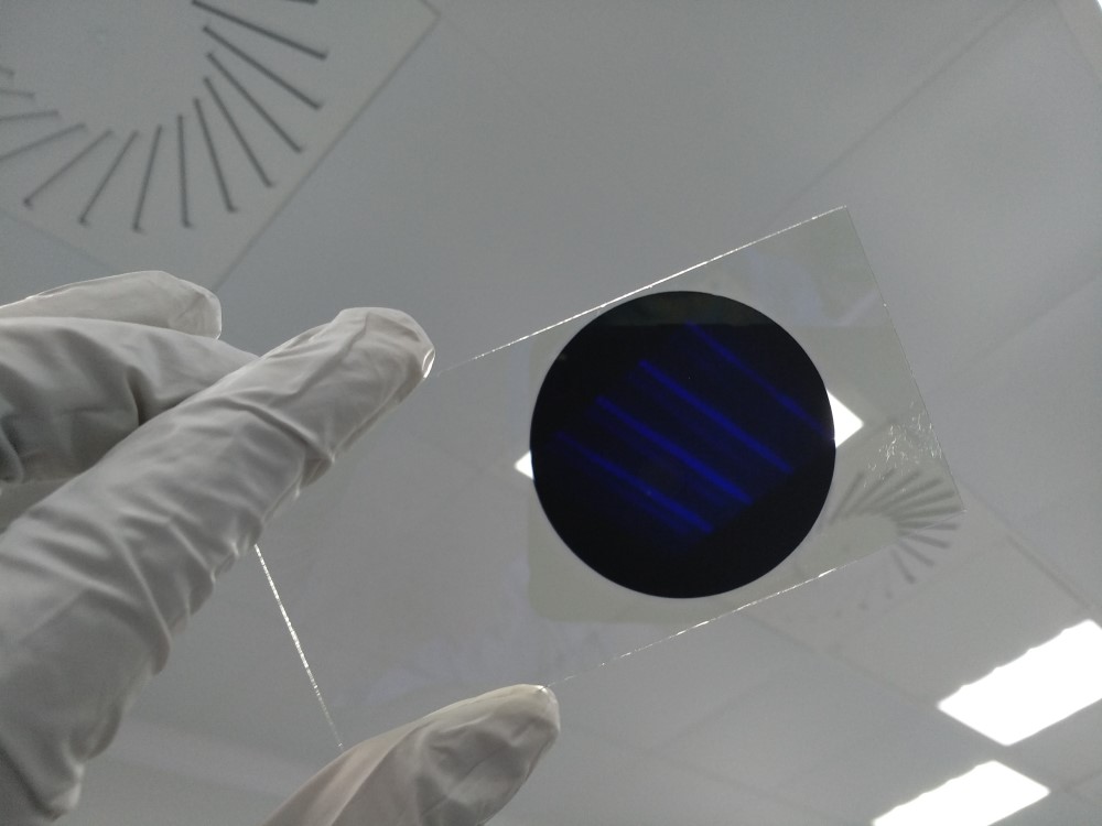
The Comberry TM infrastructure can be utilized for PVD deposition to create thin-films and thin-film devices for customer needs.

Measurements

The Comberry TM team has all the necessary competencies to conduct comprehensive metrological analysis of customer samples. 


Participation in research and development together with scientific institutions, development of research projects

The Comberry TM team using its own  infrastructure can be an R&D developer, providing services for PVD deposition, selection and measurement of materials for thin-film devices, device testing.

Also, the Comberry TM infrastructure can be provided to scientific institutions to perform their work.

Licensing and technology transfer

The Comberry TM team performs both its own and custom development projects, the rights to which can be transferred or licensed to interested individuals or legal entities.

Creation of production facilities using own technologies

The Comberry TM team has been developing several own startup projects based on our own technologies. We are interested in investors and industrial partners for further development of projects  .

COMBERRY

About us

The Comberry ™ Technology Platform is an R&D infrastructure for accelerated development of multifunctional thin-films for glass, ceramics, metals and polymers.

Comberry was established, by the Nanocenters of Dubna, Ulyanovsk and Saransk jointly with Intermolecular Inc., in October 2013. 

Product:

- applied research in the field of multifunctional thin-film coatings for various materials.

The Comberry TM mission:

To provide innovative Russian companies with technological development capabilities, poised to allow them to become successful producers of high-tech products.

Collaborative development programs allow Comberry TM customers to increase applied R&D efficiency and create large number of IP objects with drastic reduction in time to market for new products.

First stage projects

- Transparent Conductive Oxides (TCO)

- Thin-film energy storage systems (Supercapacitor of Thinika)

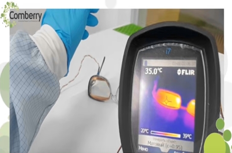
- Electrochromic devices by the TUNOX technology


Participants
Team
  • Elena
    Kolesnikova
    Chemical Engineer

    In 2007 obtained a Bachelor Degree in Technology of Semiconductor Materials (Lomonosov Moscow State University of Fine Chemical Technology).

    In 2009 graduated from Lomonosov Moscow State University of Fine Chemical Technologies with an Engineer Degree in Material Science and Technology of Advanced Materials.

    Studied English in Great Britain and passed Test of English as a Foreign Language (TOEFL). 

    Her work experience includes an engineering position with Orion Research –And-Production Association (Moscow) and a process-engineer II position with Composite in the city of Korolev.

    In 2014 as part of the Comberry-Intermolecular Joint Development Program, she interned at Intermolecular, Inc., USA, concentrating on analysis techniques and technologies for creating thin films through Wet Process.
     

  • Vladimir
    Meshcheryakov
    Project Manager / Manufacturing Engineer

    In 1999 graduated from Lomonosov Moscow State University (MSU), Department of Chemistry with a degree in chemistry. Since 1996 conducted scientific experiments in the laboratory of π-complexes of transition metals at the A.N. Nesmeyanov Institute of Organoelement Compounds of the Russian Academy of Sciences. Received a Ph.D. in chemistry of organometallic and metallacarborane compounds at the A.N. Nesmeyanov Institute of Organoelement Compounds of Russian Academy of Sciences. After defending his dissertation worked as a research fellow in Northern Illinois University (Illinois, USA), Southern Methodist University (Texas, USA), University of the Free State (Free State, South Africa), and Stellenbosch University (Western Cape, South Africa). He was the Head of the Chemistry Division of the FSUE “Research Institute of Applied Acoustics” (Dubna, Russia) and the head of the Research and Production Center PK CedRus (Kolomna, Russia).
  • Mikhail
    Ermakov
    Engineer

    In 2009 graduated from Ulyanovsk State University, Faculty of Physics and High Technology Engineering with a degree in Physics. In 2007 Mikhail started working in the Engineering Physics Department (former Optics and Solid-State Spectroscopy Department). Defended his PhD dissertation on Semiconductor Physics. Previously worked in the Federal Research-and-Production Center JSC “Research-and-Production Association “Mars”.

  • Igor
    Lukin
    BDO
Gallery
Photo and Video
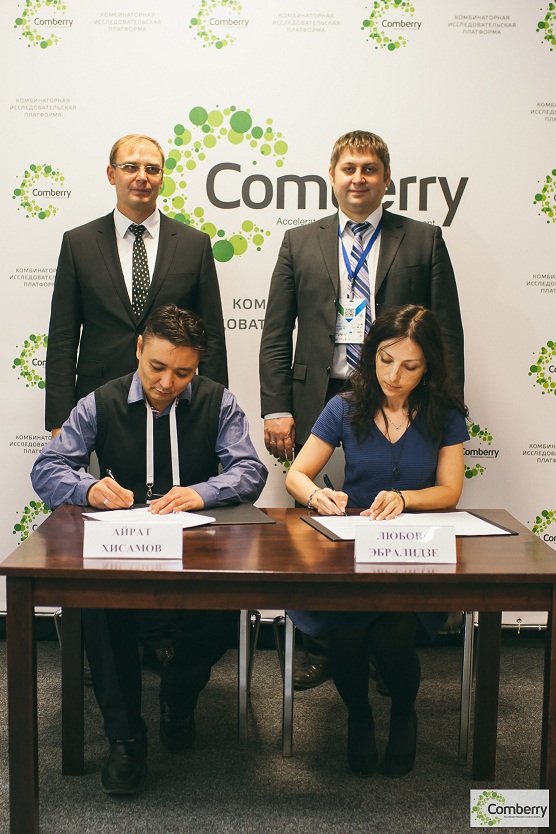
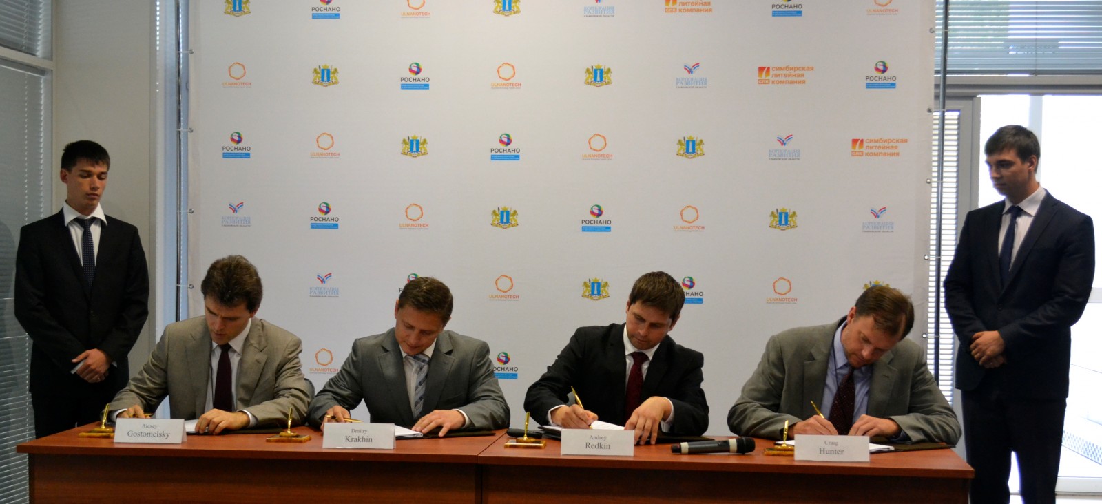
  • Signing of an agreement to establish a technology company in the Ulyanovsk region specializing in functional thin-film coatings.
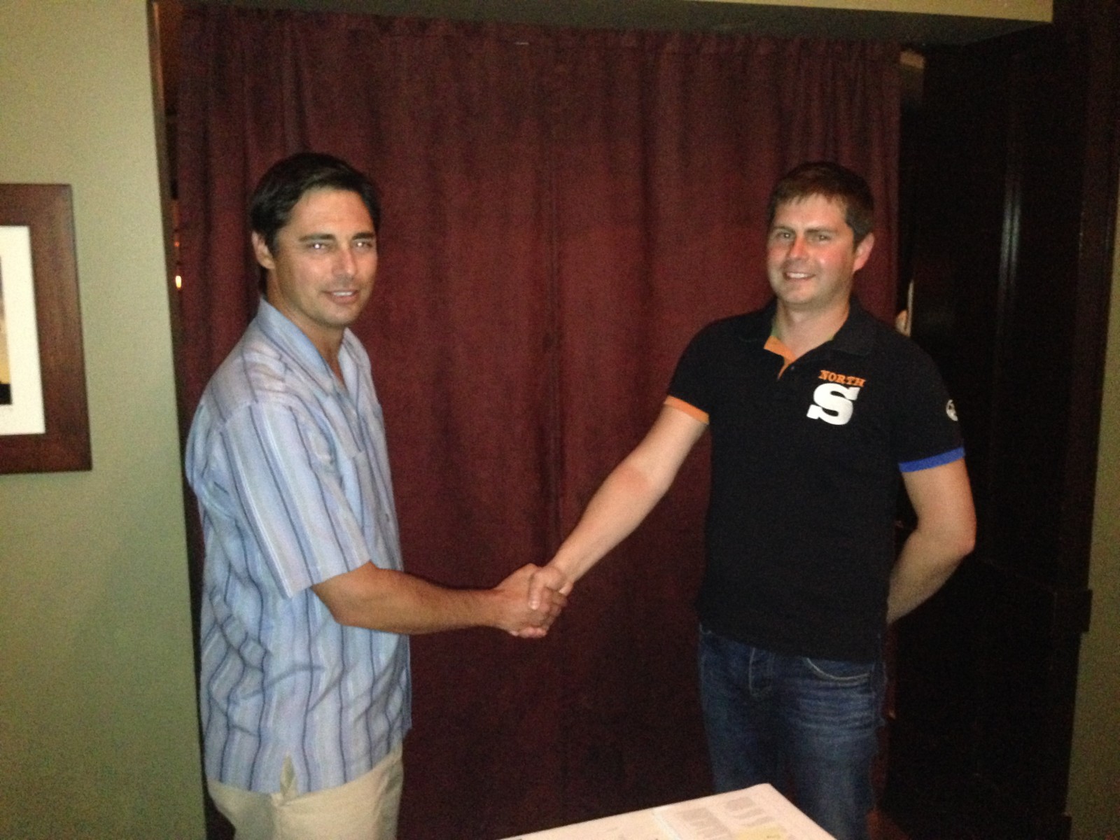
  • Signing of a joint agreement for the development of innovative solutions in functional thin-film coatings, San Jose (California, USA).
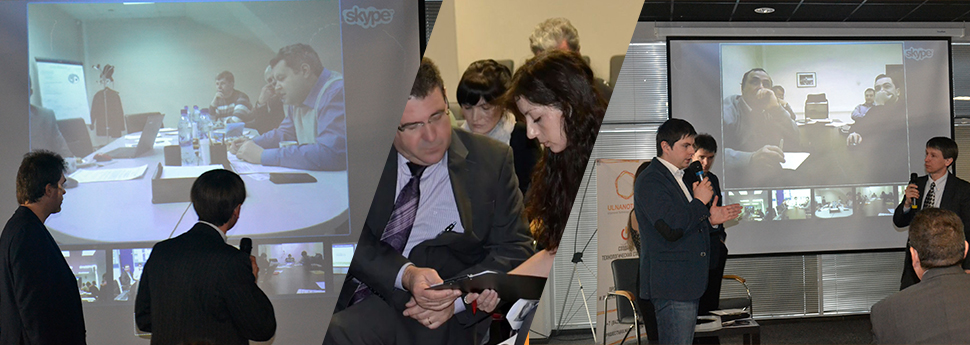
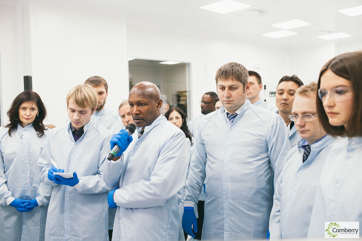
  • International Seminar across Seven RUSNANO Nanocenters
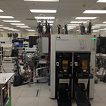
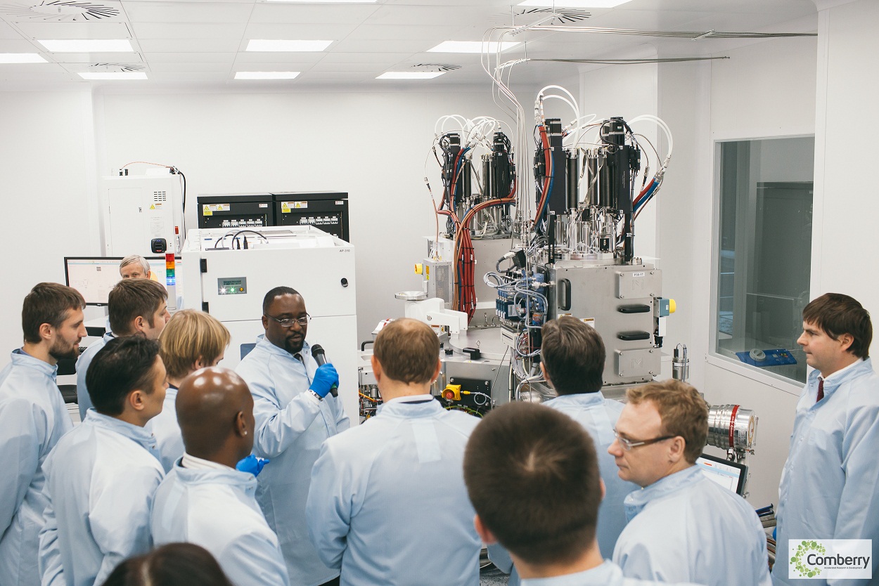
  • Intermolecular’s Laboratory
  • Tempus F-20 Reactor
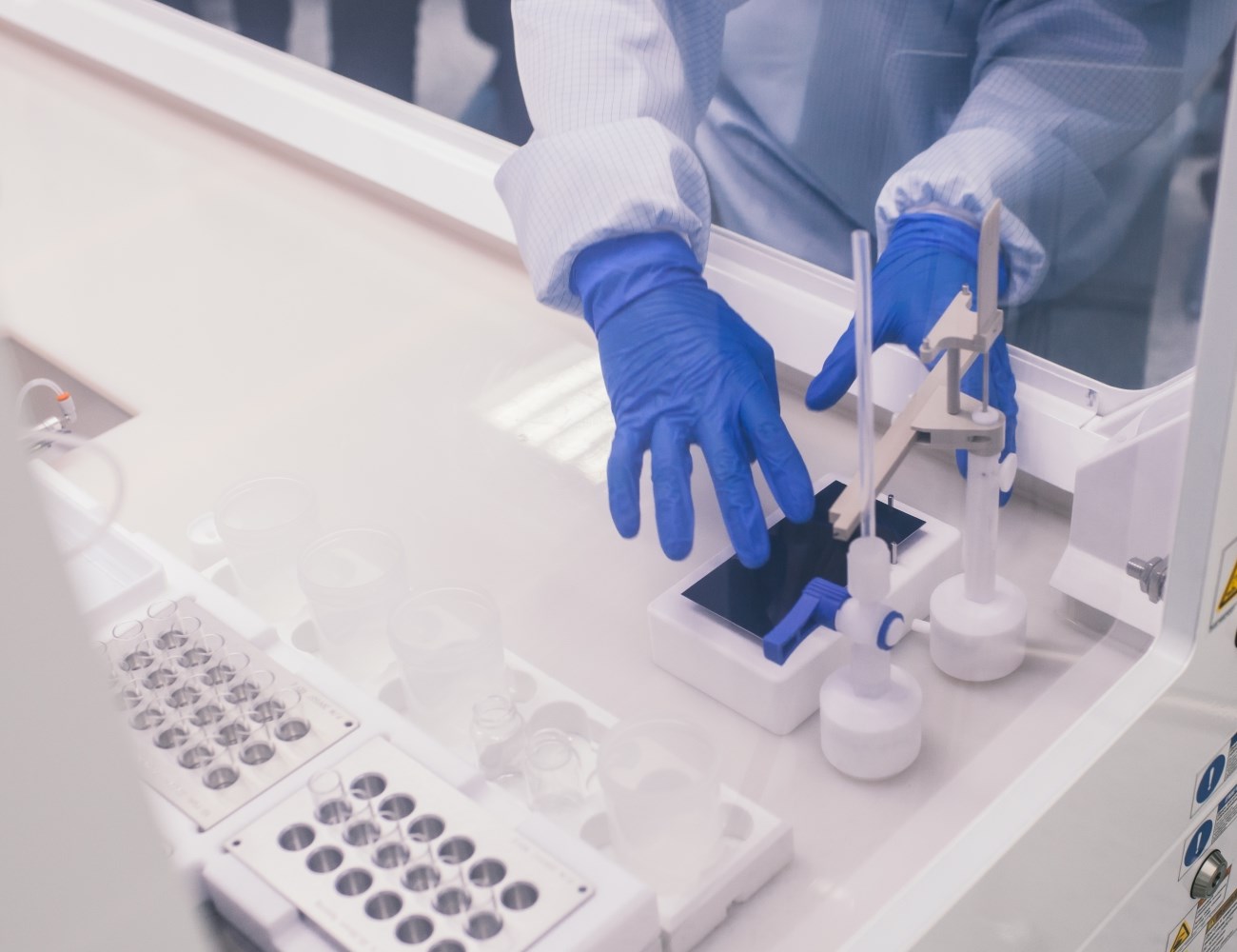
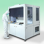
  • Tempus® F-20 Automated Combined Liquid-Processing Unit
  • Видео 1
  • Видео 2
  • Видео 3
  • Video_left1
  • Video_left2
Releases
Contact information
  • +54° 22' 7.32", +48° 40' 46.56"
  • 433400 Russia, Ulyanovskaya Oblast, Cherdaklinskiy Rayon Industrial Park “Zavolzhye”, 44 Inzhenerniy proyezd # 9
  • +7 (8422) 37 01 01

433400 Russia, Ulyanovskaya Oblast, Cherdaklinskiy Rayon Industrial Park “Zavolzhye”, 44 Inzhenerniy proyezd # 9

+7 (8422) 37 01 01

info@comberry.ru

Join the Consortium
  • * - required to be filled